1. HPM6750EVK2
1.1. Overview
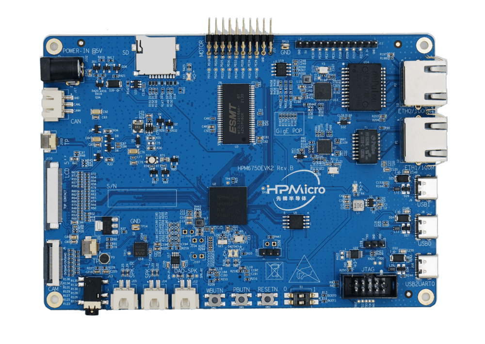
The HPM6750 is a dual-core flashless MCU running 816Mhz. It has a 2MB continuous on-chip ram. Also, it provides various memory interfaces, including SDRAM, Quad SPI NOR Flash, SD/eMMC. It integrates rich audio and video interfaces, including LCD, pixel DMA, camera, and I2S audio interfaces.
1.2. Hardware
HPM6750IVM MCU (816MHz, 2MB OCRAM)
Onboard Memory
256Mb SDRAM
128Mb Quad SPI NOR Flash
Display & Camera
LCD connector
Camera (DVP)
Ethernet
1000 Mbits PHY
100 Mbits PHY
USB
USB type C (USB 2.0 OTG) connector x3
Audio
Line in
Mic
DAO
Others
TF Slot
RGB LED
CAN
Expansion port
Motor control
1.3. DIP Switch S1
Bit 1 and 2 controls boot mode
bit[2:1] |
Description |
|---|---|
OFF, OFF |
Boot from Quad SPI NOR flash |
OFF, ON |
Serial boot |
ON, OFF |
ISP |
1.5. Plug-in
The ADC/DAC reference voltage is selected as follows:
Connection
Description
J108[2, 3]
Reference voltage
1.6. Resistor Switch
GigE POP
R177-R182Status
Description
Welding
Network
Disconnect
Motor
1.7. Pin Description
UART0 Pin:
The UART0 pin leads to three positions:
Function |
Pin |
Position1 |
Position2 |
Position3 |
|---|---|---|---|---|
UART0.TX |
PY06 |
J109[1] |
JTAG P4[7] |
USB2UART0 |
UART0.RX |
PY07 |
J109[3] |
JTAG P4[9] |
USB2UART0 |
**Note:**To avoid abnormal functions caused by multiple connections, please ensure that there is only one connection. For example, if the JTAG interface is connected to UART0, USB2UART0 interface send data to UART0 will be abnormal.
UART13 Pin:
The UART13 is used for core1 debug console or some functional testing using UART, such as uart_software_rx_idle, uart_rx_timeout, uart_software_lin, MICROROS_UART, USB_CDC_ACM_UART, MODBUS_RTU etc.
Function |
Pin |
Position |
Remark |
|---|---|---|---|
UART13.TXD |
PZ09 |
J11[5] |
|
UART13.RXD |
PZ08 |
J11[6] |
|
UART13.break |
PE31 |
J11[7] |
generate uart break signal |
TRGMUX pin for uart_software_rx_idle sample
Function |
Position |
|---|---|
TRGM2_P9(PD19) |
J10[20] |
SPI Pin:
Function |
Pin |
Position |
|---|---|---|
SPI2.CSN |
PE31 |
J11[7] |
SPI2.SCLK |
PE27 |
J11[8] |
SPI2.MISO |
PE28 |
J11[9] |
SPI2.MOSI |
PE30 |
J11[10] |
I2C Pin::
Function |
Pin |
Position |
|---|---|---|
I2C0.SCL |
PZ11 |
J11[3] |
I2C0.SDA |
PZ10 |
J11[4] |
PWM Pin:
Function |
Pin |
Position |
|---|---|---|
PWM2.P[0] |
PD31 |
J10[14] |
PWM2.P[1] |
PD30 |
J10[13] |
ACMP Pin
Function |
Pin |
Position |
|---|---|---|
CMP.INN6 |
PE21 |
J10[8] |
CMP.COMP_1 |
PE25 |
J10[6] |
GPTMR Pin
Function |
Pin |
Position |
Remark |
|---|---|---|---|
GPTMR4.CAPT_1 |
PE25 |
J10[6] |
|
GPTMR3.COMP_1 |
PE24 |
J10[8] |
MCLK of i2s emulation |
GPTMR5.COMP_2 |
PD24 |
J10[18] |
LRCK of i2s emulation |
GPTMR5.COMP_3 |
PD23 |
J10[16] |
BLCK of i2s emulation |
ADC12 Pin
Function |
Pin |
Position |
|---|---|---|
Reference Voltage |
VREFH |
J108[2] |
ADC0.VINP11 |
PE25 |
J10[6] |
ADC16 Pin
Function |
Pin |
Position |
|---|---|---|
Reference Voltage |
VREFH |
J108[2] |
ADC3.INA2 |
PE29 |
J10[5] |
headphone interface
Function |
Position |
Standard |
|---|---|---|
3.5mm headphone |
J13 |
OMTP |
audio input interface
Function |
Position |
|---|---|
microphone |
P3 |
DAO interface
Function |
Position |
|---|---|
DAO-SPK |
J12 |
Ethernet PPS Pin
Function |
Pin |
Position |
|---|---|---|
ENET0.EVTO0 |
PF05 |
U11[3] |
ENET0.EVTI1 |
PE25 |
J10[6] |
Motor Pin:
Need to remove all the resistors selected by
GigEPOPsilkscreen and make sure all the resistors selected byMOTOR POPsilkscreen are soldered, the development board list is as follows.Using the high-frequency injection demo, need to remove PWM ground resistors R436-R441.
Refer to section DRV-LV50A-MP1907 Motor Driver Board for configuration
Tamper Pin
Function |
Pin |
Position |
Mode |
|---|---|---|---|
TAMP.08 |
PZ08 |
J11[6] |
Active Mode |
TAMP.09 |
PZ09 |
J11[5] |
Active Mode |
TAMP.10 |
PZ10 |
J11[4] |
Passive Mode |
CS Pin of i2s emulation
Function |
Position |
Remark |
|---|---|---|
PD25 |
J10[16] |
the pin that controls the SPI slave CS |