8. HPM6E00EVK
8.1. Overview
The HPM6E00 is a dual-core MCU running 600MHz, with high computing power and abundant peripheral resources, and 2MB of RAM on the chip.
The HPM6E00EVK is an evaluation board for the HPM6E00 series MCU, providing a range of interfaces including ADC input with SMA interface, SDM input with SMA interface, motor control interface (QEO/QEI/SEI/PWM/ADC), CAN interface, Ethernet interface, EtherCAT interfaces, USB interface, audio interface, PPI/FREMC interface, and Raspberry Pi interface. It also integrates an onboard debugger FT2232 for easy debugging by users.
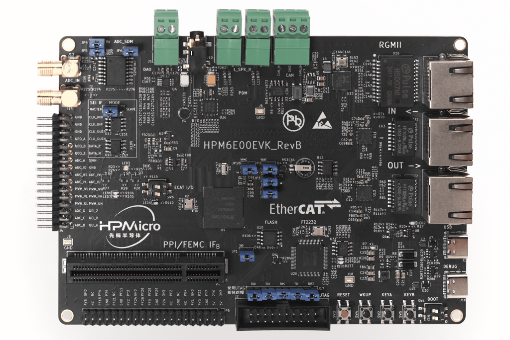
8.2. Hardware
HPM6E00 MCU (600MHz dual-core, 2MB onchip RAM)
Onboard Memory
16MB Quad SPI NOR Flash
Ethernet
1000 Mbits PHY
Ethercat
2 port
USB
USB type C (USB 2.0 OTG) connector x1
Audio
Line in
Mic
DAO
Motor
RS422
RS485
AD sensor
NSI1306W25
Others
RGB LED
CAN
Attention
When using FEMC(SDRAM) or PPI peripherals, please insert the corresponding expansion board into the PPI/FEMC interface
The standard expansion board for HPM6E00EVK evaluation purposes is as follows, with a 16 bits SDRAM (FEMC access) and a parallel ADC (PPI access).
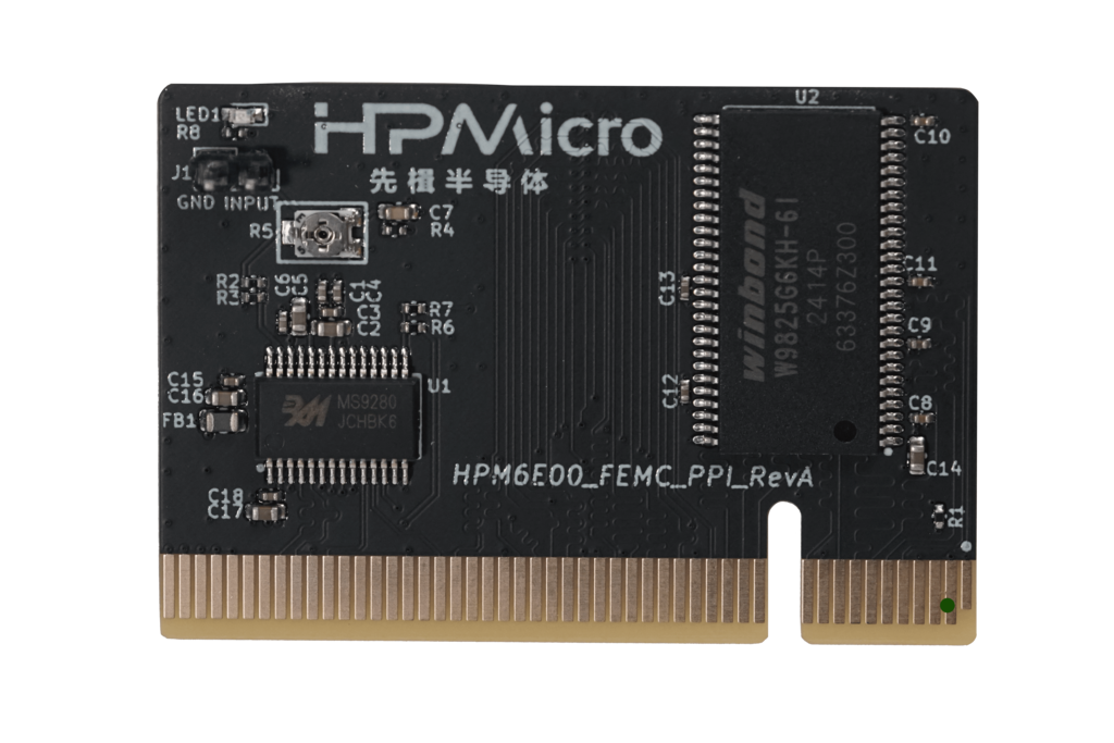
The FEMC/PPI interface has high flexibility. If you need to evaluate other parallel port devices, such as FPGA, ASYNC SRAM, etc., you can design your own expansion board or contact us.
When using SDM peripheral and AD sensor(NSI1306W25) on board, please connect JP4、JP5、JP6 and disconnect J3
The board level SEI interface CLK pin is the same as the SDM sampling chip CLK pin and cannot be used simultaneously. Please disconnect J3 when using the SDM sampling chip; When using the SEI interface, disconnect JP6.
8.3. DIP Switch SW2
Bit 1 and 2 controls boot mode
bit[2:1] |
Description |
|---|---|
OFF, OFF |
Boot from Quad SPI NOR flash |
ON, OFF |
ISP |
8.5. Plug-in
SEI CLK Section:
Function |
Position |
Note |
|---|---|---|
SEI.CLK Section |
J3 |
Master side, CLKO active. Slave side,CLKI active |
Debug interface select
Function |
Position |
Note |
|---|---|---|
Debug interface select |
J17 |
All connected:use the on-board ft2232, All disconnected: use JTAG interface |
PPI/FEMC interface
Function |
Position |
Note |
|---|---|---|
PPI/FEMC interface |
CN1 |
Connecting to PPI or FEMC expansion board |
8.6. Pin Description
PUART Pin: The PUART is used for low power mode testing, such as wakeup, etc.
Function |
Pin |
Position |
|---|---|---|
PUART.TX |
PY0 |
P5[8] |
PUART.RX |
PY1 |
P5[10] |
UART0 Pin:
The UART0 use for core0 debugger console:
Function |
Pin |
Position |
|---|---|---|
UART0.TX |
PA00 |
DEBUGUART0 |
UART0.RX |
PA01 |
DEBUGUART0 |
UART1 Pin:
The UART1 is used for core1 debugger console or some functional testing using UART, such as MICROROS_UART, USB_CDC_ACM_UART, MODBUS_RTU, lin etc.
Function |
Pin |
Position |
Remark |
|---|---|---|---|
UART1.TX |
PY07 |
P5[5] |
|
UART1.RX |
PY06 |
P5[3] |
|
UART1.break |
PF27 |
J4[6] |
generate uart break signal |
CAN Pin
Function |
Postion |
|---|---|
CAN_H |
J7[0] |
CAN_L |
J7[2] |
Audio Pin
Function |
Postion |
|---|---|
Speaker Left Channel |
J11 |
Speaker Right Channel |
J12 |
3.5mm |
J10 |
DAO Interface |
J5 |
ADC Pin
Function |
Postion |
|---|---|
ADC Input |
J4[2] |
SDM ADC Input |
J13 |
ACMP pin
Function |
Position |
|---|---|
CMP0.INN4 |
J4[18] |
Quadrature Encoder Pin
Function |
Postion |
|---|---|
QEI.A / HALL.U |
J4[1] |
QEI.B / HALL.V |
J4[3] |
QEI.Z / HALL.W |
J4[5] |
QEO.A |
J4[26] |
QEO.B |
J4[24] |
QEO.Z |
J4[22] |
PWM Output Pin
Function |
Postion |
|---|---|
PWM.WL |
J4[12] |
PWM.WH |
J4[11] |
PWM.VL / PWM1.P3 |
J4[10] |
PWM.VH / PWM1.P2 |
J4[9] |
PWM.UL / PWM1.P1 |
J4[8] |
PWM.UH / PWM1.P0 |
J4[7] |
SEI Pin
Function |
Postion |
Note |
|---|---|---|
SEI.CLK_IN_P |
J4[29] |
Clock differential output in host mode P |
SEI.CLK_IN_N |
J4[31] |
Clock differential output in host mode N |
SEI.CLK_OUT_P |
J4[27] |
Clock differential input in slave mode P |
SEI.CLK_OUT_N |
J4[25] |
Clock differential input in slave mode N |
SEI.DATA_P |
J4[23] |
Data differential Signal P |
SEI.DATA_N |
J4[21] |
Data differential Signal N |
QEIV2 Sin/Cos Pin
Function |
Postion |
Note |
|---|---|---|
ADC2.INA11 |
J4[15] |
ADC_IW (Cos) |
ADC0.INA14 |
J4[13] |
ADC_IU (Sin) |
RDC pin
Function |
EVK board Position |
RDC board Position |
|---|---|---|
RDC.PWM |
J4[7] |
J2[7] |
RDC.ADC0 |
J4[13] |
J2[13] |
RDC.ADC1 |
J4[14] |
J2[14] |
GND |
J4[32] |
J2[17] |
PLB Pin | Function | Postion | | PLB.PULSE_OUT | J4[5] |
Tamper Pin
Function |
Pin |
Position |
Mode |
|---|---|---|---|
TAMP.04 |
PZ04 |
P5[18] |
Active Mode |
TAMP.05 |
PZ05 |
P5[33] |
Active Mode |
TAMP.03 |
PZ03 |
P5[7] |
Passive Mode |
LOBS Pin
Pin |
Position |
|---|---|
PF26 |
P5[23] |
GPTMR Pin:
Function |
Position |
Remark |
|---|---|---|
GPTMR4.CAPT_0 |
J4[3] |
|
GPTMR4.COMP_0 |
J4[1] |
BLCK of i2s emulation |
GPTMR0.COMP_0 |
J4[26] |
LRCK of i2s emulation |
GPTMR5.COMP_2 |
J4[5] |
MCLK of i2s emulation |
CS Pin of i2s emulation
Function |
Position |
Remark |
|---|---|---|
PA11 |
P1[4] |
the pin that controls the SPI slave CS |
SPI Pin:
Function |
Pin |
Position |
|---|---|---|
SPI7.CSN |
PF27 |
J4[6] |
SPI7.SCLK |
PF26 |
P5[23] |
SPI7.MISO |
PF28 |
P5[21] |
SPI7.MOSI |
PF29 |
P5[19] |
I2C Pin:
Function |
Position |
|---|---|
I2C0.SCL |
P5[28] |
I2C0.SDA |
P5[27] |
Ethernet PPS PPS Pin:
Function |
Pin |
Position |
|---|---|---|
ENET0.EVTO0 |
PE06 |
J4[24] |
ENET0.EVTO1 |
PF20 |
J4[4] |
ENET0.EVTI1 |
PE07 |
J4[26] |
ECAT:
Function |
Pin |
Position |
|---|---|---|
Port0 |
- |
P1 |
Port1 |
- |
P2 |
RUN LED |
PE03 |
LED7 |
ERR LED |
PE02 |
LED6 |
Input IO(2bit) |
PC31/PD09 |
SW6 |
Output IO(2bit) |
PD08/PE14 |
LED8/LED3 |