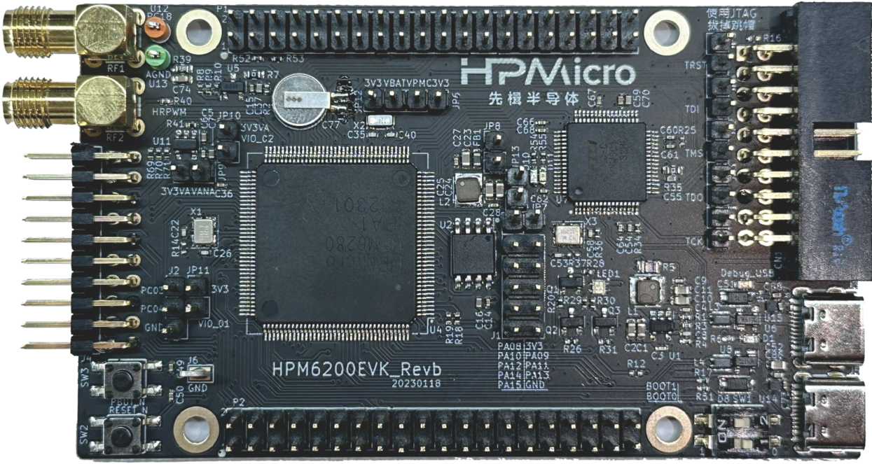
3. HPM6200EVK
3.1. Overview
The HPM6200EVK provides a series of interfaces for the characteristic peripherals of the HPM6200 series microcontrollers, including an ADC input SMA interface, a high-resolution PWM output SMA interface, and a first-class motor control interface. HPM6200EVK also integrates two 2x20 pin IO expansion interfaces, which connect most of the IOs of HPM6200 MCU for users to freely evaluate. HPM6200EVK expands NOR Flash storage for MCU and integrates an on-board debugger.
3.2. DIP Switch SW1
bit[2:1] |
Description |
|---|---|
OFF, OFF |
Boot from Quad SPI NOR flash |
OFF, ON |
Serial boot |
ON, OFF |
ISP |
3.4. Pin Description
UART pin
The UART2 is used for core1 debug console or some functional testing using UART, such as MICROROS_UART, USB_CDC_ACM_UART, MODBUS_RTU etc.
Function
Position
Remark
UART2.TXD
P1[8]
UART2.RXD
P1[10]
UART2.break
P2[29]
generate uart break signal
LIN Pin:
Function
Position
LIN0.TX
J1[3]
LIN0.RX
J1[6]
SDM Pin:
Function
Position
SDM0.CLK_3
P2[27]
SDM0.DAT_3
P2[28]
SPI Pin:
Function
Position
SPI1.CSN
P2[29]
SPI1.SCLK
P2[32]
SPI1.MISO
P2[31]
SPI1.MOSI
P2[33]
I2C Pin:
Function
Position
I2C0.SCL
P2[7]
I2C0.SDA
P2[10]
ACMP Pin:
Function
Position
ACMP.CMP1.INN5
J4[6]
ACMP.COMP_1
J4[8]
GPTMR Pin:
Function
Position
Remark
GPTMR1.CAPT_0
P2[3]
GPTMR1.COMP_0
P2[23]
MCLK of i2s emulation
GPTMR1.COMP_1
P2[24]
LRCK of i2s emulation
GPTMR1.COMP_2
P2[5]
BLCK of i2s emulation
ADC16 Pin:
Function
Position
ADC0.INA8
P2[11]
DAC Pin:
Function
Position
DAC0.OUT
J2[1]
DAC1.OUT
J2[2]
PWM Pin:
Function
Position
PWM0.P0
J4[14]
PWM0.P1
J4[13]
HRPWM Pin:
Function
Position
HRPWM0.P0
RF2
HRPWM0.P2
P2[29]
PLA Output Pin:
Function
Position
PLA.OUT
P1[26]
Motor Pin:
Refer to section DRV-LV50A-MP1907 Motor Driver Board for configuration
The HALL pin of the hpm6200evk needs to be connected.
HALL Pin:
Function
EVK Position
Motor Position
HALL.U
J4[20]
J22[3]
HALL.V
J4[18]
J22[4]
HALL.W
J4[16]
J22[5]
GND
J4[4]
J22[1]
Tamper Pin
Function
Pin
Position
Mode
TAMP.04
PZ04
P1[33]
Active Mode
TAMP.05
PZ05
P1[36]
Active Mode
TAMP.06
PZ06
P1[38]
Passive Mode
CS Pin of i2s emulation
Function
Position
Remark
PB31
P1[7]
the pin that controls the SPI slave CS
3.5. Board Know Issue
USB VBUS pin resistance issue
Impact
This issue may affect the Host’s ability to enumerate USB as a device.
Solution
Replace the 1kohm resistors R17 with 10ohm resistors.
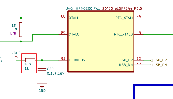
Revised Status
HPM6200EVKRevC has been revised, HPM6200EVKRevB and previous versions have this issue.